What is Inter-Integrated Circuit (I2C)?

How I2C Communication Works and How To Use It with Arduino
| Topics covered in this article: |
| Ⅰ. What is I2C? |
| Ⅱ. A brief history of I2C |
| Ⅲ. I2C basic content |
| Ⅳ. I2C bus development and design need to pay attention |
| Ⅴ. Design example |
| Ⅵ. Summary |
Ⅰ. What is I2C?
Philips invented the I2C bus, which is a simple bidirectional two-wire synchronous serial bus. Only two wires are required to convey data between devices connected to the bus.
The master device is used to open the device for transmission and to start the bus for data transmission. Any addressed device is treated as a slave device at this moment. On the bus, the relationship between master and slave, sending and receiving data is not constant, but it does rely on the data transfer direction at the time. If the host wishes to send data to the slave device, it addresses the slave device first, then actively transfers data to the slave device, and finally concludes the data transfer; if the host wants to receive data from the slave device, the master device addresses the slave device first. The host then receives the data delivered by the device before terminating the receiving operation. under these conditions. The time clock is generated by the host, and the data transfer is terminated by the host.
Ⅱ. A Brief History of I2C
In 1980, Philips began to develop a communication bus in order to connect various low-speed devices (Philips chips).
In 1982, the original version used a 100KHz communication rate, provided 7-bit addresses, and limited the number of devices on the bus to 112 (with several reserved addresses).
In 1992, the first specification was published, adding a fast mode of 400kHz and an expanded 10-bit address space.
In 1998, with the advancement of technology, the communication rate requirements became higher and higher, reaching a high-speed 3.4 MHz, and then upgraded to 5 MHz later, and differential signals were used to improve noise immunity.
Ⅲ. I2C basic content
I²C: Inter-Integrated Circuit, which literally means between integrated circuits, is the abbreviation of I²C Bus.
I2C requires only two wires, which can support up to 1008 slave devices for synchronous serial communication.
Unlike SPI , I2C can support multi-master, multi-slave bus.

I2C
I2C two-wire signal
Each I2C bus is made up of two signals: SCL clock and SDA data. The present bus master generates the clock signal at all times.
I 2 C bus drivers, unlike UART and SPI, are open-drain (please Google if you don't know what open-drain means), which means they can draw the appropriate signal line low but not drive it high.
When no device is pushing the signal low, a pull-up resistor on each signal line returns it to a high level.

Signal of I2C
Signal level
The I2C bus signal level is usually between 5 and 3.3 volts. The device on the bus can be utilized directly if it is compatible with these two levels.
Level conversion is essential if the signal voltages are substantially different (5V and 2.5V), or if the levels are not compatible.
Ⅳ. I2C bus development and design need to pay attention
1. Bus capacity and drive capability
Because the I2C bus's peripheral expansion devices are all CMOS devices and the bus has sufficient current drive capability, the number of nodes extended on the bus is determined by the capacitive load rather than the current load capabilities.
Each actual node device on the bus has an equivalent capacitance at its bus interface. Because of the analogous capacitance, bus transmission will be delayed, resulting in data transmission mistakes.
The bus load capacity is typically 400pF, and each I2C device has its own capacitance value, usually no more than 20pF, from which the bus length and number of nodes may be estimated. Because each peripheral device on the bus has a device address, the device address also limits the expansion of peripheral devices on the bus.
2. The electrical structure of the I2C bus
The internal I2C bus interface is a bidirectional transmission circuit, as indicated in the picture, because the I2C bus is a bidirectional synchronous serial bus. Because the bus port's output has an open-drain structure, a pull-up resistor must be installed on the bus. The power supply voltage, SDA, SCL, and the bus series resistance are all affected by the pull-up resistor, For selection, refer to the applicable data sheet, which normally ranges from 4.7K to 10K.

Typical Application
3. Each node has a fixed node address.
Because the I2C bus is a bidirectional synchronous serial system, a single-chip microcomputer on the bus can act as the master node, with its device address given by software and saved in the bus's address register, which is referred to as the slave address of the master device. When a single-chip microcomputer is used as a slave node in a multi-master bus system, its slave address is meaningful, resulting in standardized device addresses for all peripheral devices on the bus.
4. I2C bus timing
Each frame of data transmitted on the I2C interface is one byte in length. However, once the bus is started, there is no limit to the amount of bytes that can be communicated; all that is required is that the other side acknowledges each byte transmitted. The most significant chunk of info is transmitted first when sending. Each transfer has a start signal at the beginning and a stop signal at the conclusion. By manipulating the clock line after the bus has transferred a byte, the transmission can be halted.
①Clock and data transmission:
An external device is commonly used to pull the SDA pin high. When SCL is low, data on the SDA pin can only be modified; when SCL is high, data on the SDA pin indicates a start or stop state. as shown in the illustration

Clock and data transmission
②Start and end conditions:
A start condition is a high-to-low SDA with SCL high that must come before any other command. A stop condition is a low-to-high SDA and SCL high. A stop instruction puts the EEPROM into standby mode after a read sequence, as shown in the diagram.

Start and end conditions
③ Answer:
All address and data words are continually sent to the EEPROM as 8-bit words, and the EEPROM confirms receipt of each word by transmitting a "0." As illustrated, the acknowledgment occurs on the ninth clock cycle.

Answer

I2C Version History
Say something extra about SMBus :
The "System Management Bus," based on I2C, was introduced by Intel in 1995. (SMBus). SMBus is a more tightly controlled format that aims to improve communication predictability between supporting ICs on PC motherboards.
The main difference between SMBus and I2C is that SMBus has a speed restriction of 10kHz to 100kHz, whereas I2C can support devices from 0kHz to 5MHz.
Ⅴ. Design example
The AT24C256 is a 256kbit serial electrically erasable programmable read-only memory from ATMEL, packaged in an 8-pin dual-row in-line device with a small construction, substantial storage capacity, and other features that may be utilized in a 2-wire bus. Connect four of these ICs in series to create a data acquisition system with high-capacity data storage requirements.

AT24C256
Data can be received and transmitted using EEPROM memory devices. Each device connected to the bus has its own unique address.
When the host accesses the EEPROM. it sends the start condition and control signal to the EEPROM memory, as well as the red flag signal to flip the direction of data transmission and receipt. The relevant data can then be read out after getting the response signal from the EEPROM,
Ⅵ. Summary
Through the above examples, we can know that the advantages of I2C are mainly manifested in:
1. The hardware circuit has been streamlined. The serial data line (SDA) and the serial clock line are the only lines required in this bus (SCL).
2. Each I2C device on the bus has a unique address that software can use to address it.
3. Because there may be numerous master I2C devices on the bus, the I2C bus interface protocol includes a conflict monitoring and arbitration mechanism to prevent data loss or communication failures.
4. The standard mode of this serial two-wire bidirectional bus is 100 kbit/s, the fast mode is 400 kbit/s, and the high-speed mode is 3.4 mbit/s.
5. The data integrity is ensured by filtering and anti-interference techniques in the I2C device.
6. The bus's capacitive reactance cannot exceed 400pF since the number of devices connected to it is limited.
1. What determines the transfer rate of I2C?
The transfer rate of the IIC is determined by the "clock frequency on the clock line (SCL)."
2. What is the maximum length of the I2C bus?
The maximum length of the I2C bus is: less than 200mm ~ 300mm, which is related to the transmission speed, wiring, etc. I2C repeater chips can be used to extend the distance, NXP such as P82B715, P82B96, etc.; there is no clear regulation on the standard for effective transmission. distance.
3. What is the difference between slave mode and master mode of I2C?
First, the subject is different
1. Slave mode: fast mode, can receive and transmit at 400kbit/s.
2. Main mode: Also known as high-speed mode, it can transmit information at a bit rate of up to 3.4Mbit/s.

Second, the characteristics are different
1. Slave mode: Adjusted the timing of serial data (SDA) and serial clock (SCL) signals.
2. Master mode: The current source circuit shortens the rise time of the SCLH signal. At any time in the Hs mode, only the current source of one master is valid.

Third, the rules are different
1. Slave mode: The power supply voltage of the fast mode device is turned off, and the I/O pins of SDA and SCL must be left floating, and the bus cannot be blocked.
2. Master Mode: Mode The master device generates a serial clock signal with a 1:2 ratio of high and low. The timing requirements for setup and hold times have been lifted.
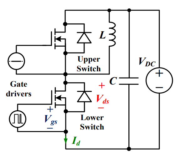 Discovering New and Advanced Methodology for Determining the Dynamic Characterization of Wide Bandgap DevicesSaumitra Jagdale15 March 20242467
For a long era, silicon has stood out as the primary material for fabricating electronic devices due to its affordability, moderate efficiency, and performance capabilities. Despite its widespread use, silicon faces several limitations that render it unsuitable for applications involving high power and elevated temperatures. As technological advancements continue and the industry demands enhanced efficiency from devices, these limitations become increasingly vivid. In the quest for electronic devices that are more potent, efficient, and compact, wide bandgap materials are emerging as a dominant player. Their superiority over silicon in crucial aspects such as efficiency, higher junction temperatures, power density, thinner drift regions, and faster switching speeds positions them as the preferred materials for the future of power electronics.
Read More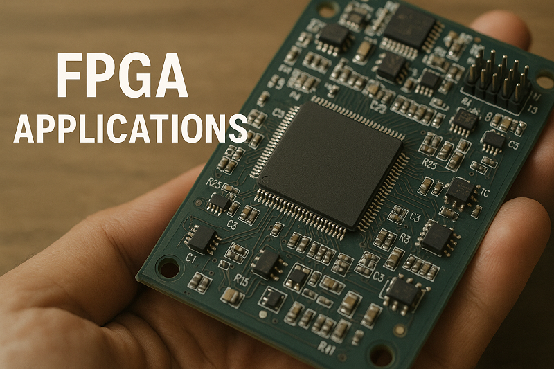 A Comprehensive Guide to FPGA Development BoardsUTMEL11 September 202514409
This comprehensive guide will take you on a journey through the fascinating world of FPGA development boards. We’ll explore what they are, how they differ from microcontrollers, and most importantly, how to choose the perfect board for your needs. Whether you’re a seasoned engineer or a curious hobbyist, prepare to unlock new possibilities in hardware design and accelerate your projects. We’ll cover everything from budget-friendly options to specialized boards for image processing, delve into popular learning paths, and even provide insights into essential software like Vivado. By the end of this article, you’ll have a clear roadmap to navigate the FPGA landscape and make informed decisions for your next groundbreaking endeavor.
Read More Applications of FPGAs in Artificial Intelligence: A Comprehensive GuideUTMEL29 August 20253580
This comprehensive guide explores FPGAs as powerful AI accelerators that offer distinct advantages over traditional GPUs and CPUs. FPGAs provide reconfigurable hardware that can be customized for specific AI workloads, delivering superior energy efficiency, ultra-low latency, and deterministic performance—particularly valuable for edge AI applications. While GPUs excel at parallel processing for training, FPGAs shine in inference tasks through their adaptability and power optimization. The document covers practical implementation challenges, including development complexity and resource constraints, while highlighting solutions like High-Level Synthesis tools and vendor-specific AI development suites from Intel and AMD/Xilinx. Real-world applications span telecommunications, healthcare, autonomous vehicles, and financial services, demonstrating FPGAs' versatility in mission-critical systems requiring real-time processing and minimal power consumption.
Read More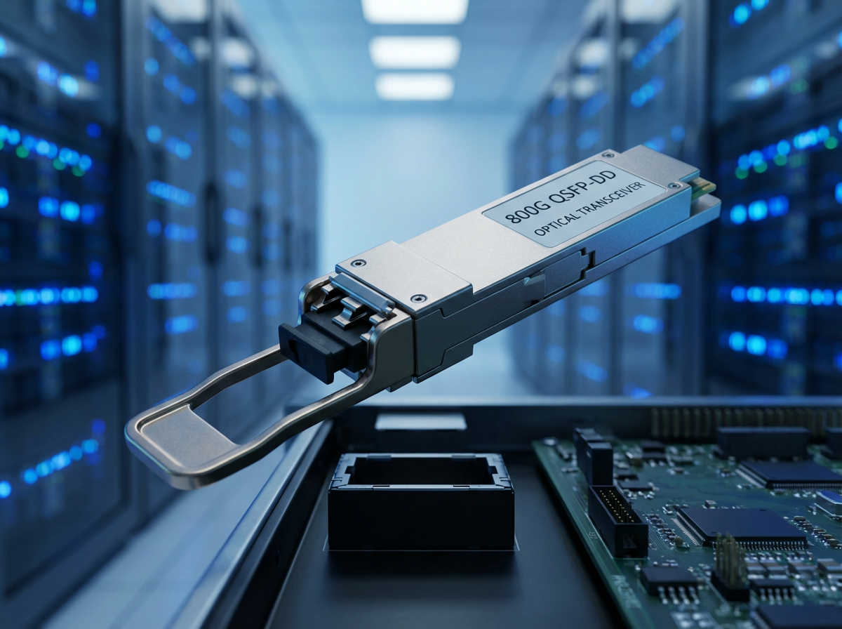 800G Optical Transceivers: The Guide for AI Data CentersUTMEL24 December 20253713
The complete guide to 800G Optical Transceiver standards (QSFP-DD vs. OSFP). Overcome supply shortages and scale your AI data center with Utmel Electronic.
Read More Xilinx FPGAs: From Getting Started to Advanced Application DevelopmentUTMEL09 September 20254273
This guide is your comprehensive roadmap to understanding and mastering the world of Xilinx FPGA technology. From selecting your first board to deploying advanced AI applications, we'll cover everything you need to know to unlock the potential of these remarkable devices. The global FPGA market is on a significant growth trajectory, expected to expand from USD 8.37 billion in 2025 to USD 17.53 billion by 2035. This surge is fueled by the relentless demand for high-performance, adaptable computing in everything from 5G networks and data centers to autonomous vehicles and the Internet of Things (IoT). This guide will walk you through the key concepts, tools, and products in the Xilinx ecosystem, ensuring you're well-equipped to be a part of this technological revolution.
Read More
Subscribe to Utmel !
![UCC21225ANPLR]() UCC21225ANPLR
UCC21225ANPLRTexas Instruments
![1EDI60I12AFXUMA1]() 1EDI60I12AFXUMA1
1EDI60I12AFXUMA1Infineon Technologies
![UCC5350MCDR]() UCC5350MCDR
UCC5350MCDRTexas Instruments
![HCS360-I/SN]() HCS360-I/SN
HCS360-I/SNMicrochip Technology
![ISO5500DW]() ISO5500DW
ISO5500DWTexas Instruments
![HCNW3120-300E]() HCNW3120-300E
HCNW3120-300EBroadcom Limited
![AT88SC0204CA-SH]() AT88SC0204CA-SH
AT88SC0204CA-SHMicrochip Technology
![CS8190EDWFR20G]() CS8190EDWFR20G
CS8190EDWFR20GON Semiconductor
![ATECC608A-MAHDA-T]() ATECC608A-MAHDA-T
ATECC608A-MAHDA-TMicrochip Technology
![ATSHA204A-MAHCZ-T]() ATSHA204A-MAHCZ-T
ATSHA204A-MAHCZ-TMicrochip Technology


 Product
 Brand
Brand Articles
 Tools
Tools


